

")
Wafers are the basis for the production of semiconductor components and play a crucial role in the electronics industry. However, which significance do different wafer sizes have and how do they influence the function of semiconductor components? In this technical article, we look at 'The Wafer 101', explain the common wafer sizes, and discuss their respective function and importance in semiconductor production.
What is a wafer?
A wafer is a thin round silicon disk that serves as the basis for the production of integrated circuits (ICs) and other semiconductor components. Various process steps such as photolithography, etching, and doping are used to structure tiny electronic components on a wafer, which are later used in electronic devices.
Common wafer sizes
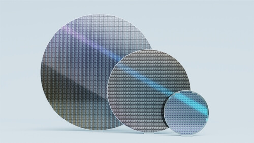
Silicon wafers are available in various diameters, which are measured in inches. The three most common sizes are:
- 6 inches (150 mm)
- 8 inches (200 mm)
- 12 inches (300 mm)
Another wafer size is 18 inches (450 mm). However, this extreme wafer size is not used in mass production, but only for research and development, as 450 mm wafers are very costly. Research facilities use 18-inch wafers to test production lines and optimize cost efficiency. The larger the wafer, the more complex the production equipment has to be.
Formerly common wafer sizes such as 2 inch (50.8 mm), 3 inch (76.2 mm), and 4 inch (100 mm) are becoming increasingly rare and have already been phased out in some cases, as the small wafers cannot cover the large production volumes or current quantities. Exceptions to this are custom-made products that are produced in small quantities, such as GaAs (gallium arsenide), SiC (silicon carbide), and InP (indium phosphide) wafers.

Function of wafer sizes
The wafer size has a direct impact on the efficiency and costs of semiconductor manufacturing. Larger wafers enable a higher yield of chips per wafer, as more components can be placed on a single wafer. This in turn leads to a more efficient production and lower unit costs per chip. For this reason, wafer sizes are of great importance in microchip production.
Challenges of extreme wafer sizes
Although large wafers offer many advantages, they also come with challenges. In the following paragraph, you will find the six most important points that can be responsible for increased susceptibility:
- Crystalline perfection and impurities
Wafers require an extremely high degree of crystalline perfection. With larger areas, the predisposition for irregularities or impurities in the crystal lattice is higher per se and therefore also the risk of defects. - Mechanical tensions
During the production and handling of larger wafers, mechanical tensions arise which can lead to fractures or cracks. These tensions are more difficult to control as larger wafers are more sensitive to mechanical stress. - Temperature gradients and thermal tensions
During manufacturing, wafers undergo several high-temperature processes. Larger wafers can have uneven temperature gradients, which can lead to thermal stress and thus defects. - Complexity of the processes
The production of semiconductor devices on larger wafers requires more complex and precise processes. The slightest deviation or error in these processes can have a greater impact over the larger area and lead to a higher defect density. - Particle contamination
As wafer size increases, so does the area that might be contaminated by particles. Even microscopically small particles can cause defects that impair the function of the semiconductor components. - Complex lithography
The lithography processes used to structure semiconductor components are more demanding with larger wafers. The slightest errors in exposure or alignment can cause defects that extend over the entire wafer surface.
The challenges mentioned above make the production of larger silicon wafers technically more demanding and increase the risk of defects, which can affect the yield and reliability of the semiconductor devices produced. This makes careful process controls and advanced manufacturing technologies all the more important to ensure the quality and reliability of semiconductor products.
The importance of wafer sizes in semiconductor manufacturing
Overall, wafer sizes play a crucial role in semiconductor manufacturing. They influence efficiency, costs, and performance of semiconductor components. Due to the continuous development and optimization of production technologies, 12-inch and 18-inch wafers are becoming increasingly important. Currently, they meet the needs of the electronics industry’s increasing requirements best. However, a comprehensive understanding of the different wafer sizes remains essential for the development and production of high-quality and future-proof electronic components.
Content Information

Editor: RoodMicrotec GmbH
Source: The text is based on information from RoodMicrotec GmbH.
Copyright: All images, videos and audio files published in this article are subject to copyright. Reproduction in whole or in part is not permitted without the written permission of RoodMicrotec GmbH.
For further information or inquiries about a joint cooperation, please contact