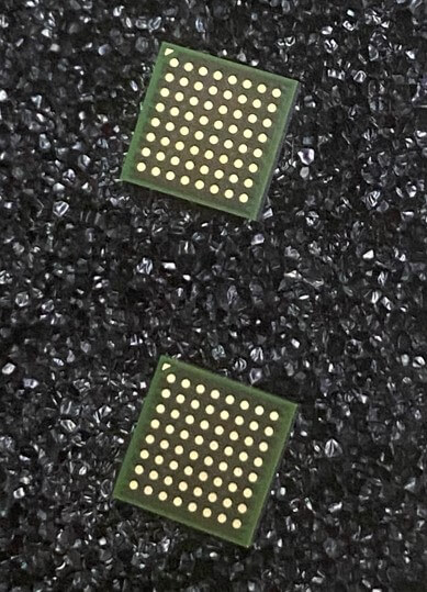
Flip chip assembly is an advanced technique in electronics manufacturing that enables the efficient and reliable mounting of semiconductor chips to printed circuit boards. In this article, we will take a closer look at flip chip assembly, explain how it works, highlight applications, and outline the benefits of this technique for the electronics industry.
What is flip chip assembly?
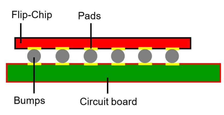
Flip chip assembly is a technique in which a chip is mounted on a printed circuit board (PCB) or substrate with its active contact surface downwards. In contrast to the conventional wire bonding technology, in which wires are used to connect the chip to the PCB, tiny solder balls (so-called 'bumps') are applied to the contact surface of the chip, which are then soldered to the corresponding pads on the PCB.
How flip chip assembly works
In flip-chip assembly, the semiconductor chip is mounted on a carrier foil or substrate with the contact surface upwards. Subsequently, small solder bumps are applied to the chip surface or the contact surface of the chip in a multi-stage coating process. These bumps have a diameter of less than 100 µm and are similar to the balls on BGA (= ball grid array) components.
This coating process is carried out either by a dispensing process or by using previously manufactured soldering devices. Once the solder balls have been applied, the chip is flipped over (hence the name 'flip chip') and positioned on the respective pads on the PCB with the solder balls downwards. Then, the solder balls are melted by heat or pressure, creating a permanent electrical connection between the chip and the circuit board.

The idea was that these chips could be soldered onto PCBs in the same reflow process as other SMD (= surface mount device) components. However, this turned out to be impractical under today's production conditions for the following reasons:
- The standard soldering paste printing process on the PCB is not precise enough.
- Automatic placement machines do not achieve the required accuracy, as they cannot "see" the component from below.
- The considerably differing expansion coefficients of silicon and PCB material lead to mechanical stresses that cannot be compensated due to the short distance between the small bumps.
This is why flip chips are only precisely placed and then immediately soldered after the other SMD components have been soldered with a special placement and soldering tool, the flip chip bonder. However, additional measures have to be taken to reduce mechanical stresses. Practical tests have shown that soldered flip chips may fail after just a short time, because the solder joints are sheared off. It is therefore essential to glue the chips additionally onto the printed circuit boards.

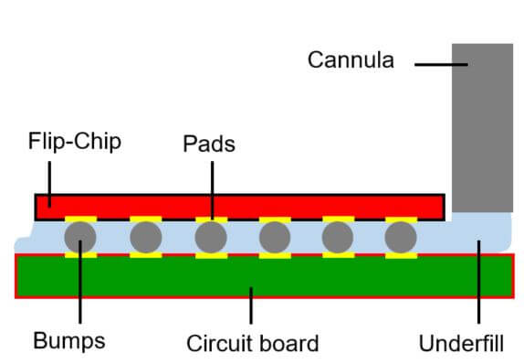
The adhesive has to flow into the narrow gap of less than 100 µm between the silicon and the PCB and encase the individual solder connections. This is achieved using a particularly low-viscosity adhesive, the so-called underfill.
The underfill material is made to flow under the chip until it emerges on the opposite side. The capillary effect ensures that the narrow gap is completely filled and bubbles or cavities are avoided. The adhesive then has to harden at medium temperatures of around 100 °C. In addition to high precision, this process also requires very high levels of purity.
As semiconductor chips are usually coated with aluminum (more recently, copper has also been used due to its better conductivity) and aluminum is difficult to solder, the application of the solder balls (the 'bumping') has to be prepared using a complex, multi-stage coating process (UBM = Under Bump Metallization). This process has to be carried out by the chip manufacturer or by highly specialized service providers and is only worthwhile for very large quantities.
Applications of flip chip assembly
Flip chip assembly is used in a variety of applications, including:
- High-performance computing: in high-performance computers and servers, flip chip assembly enables an efficient heat dissipation and a high signal integrity, resulting in improved performance and reliability.
- Telecommunications: In the telecommunications industry, flip chip assembly is used to manufacture radio frequency modules, signal processing units, and wireless communication devices.
- Automotive: In the automotive industry, flip chip assembly is used to manufacture control units, sensors, and camera systems to ensure a reliable performance under extreme conditions.
- Medical: In the medical industry, flip chip assembly is used in the production of implants, diagnostic devices, and medical imaging systems to ensure a precise and reliable functionality.
Advantages of flip chip assembly
Flip chip mounting offers a number of advantages over conventional mounting techniques, including:
- Higher packing density: by mounting the chip with the contact surfaces downwards, more connections can be placed onto a smaller area, resulting in a higher packing density and a more compact design.
- Better heat dissipation: Flip chip mounting allows heat to dissipate directly from the back of the chip to the PCB, creating a more efficient cooling for an improved performance.
- Lower signal loss: The shorter connections lengths as well as the direct contact between chip and PCB reduce signal losses and improve signal integrity.
- Higher reliability: Flip chip mounting provides a mechanically robust connection and reduces the sensitivity to vibration and mechanical stress, resulting in a higher reliability and a longer board life.
Flip chip assembly as a key technology in electronics production
Flip chip assembly is an innovative and versatile technology that is used in a wide range of applications and offers numerous advantages. Its ability to increase packing density, improve heat dissipation, reduce signal loss, and increase reliability makes it a key technology in electronics manufacturing. Through continuous research and development, flip chip assembly will continue to help improve the performance and reliability of electronic devices and drive innovation in the electronics industry.
Content Information

Editor: RoodMicrotec GmbH
Source: The text is based on information from RoodMicrotec GmbH.
Copyright: All images, videos and audio files published in this article are subject to copyright. Reproduction in whole or in part is not permitted without the written permission of RoodMicrotec GmbH.
For further information or inquiries about a joint cooperation, please contact


