

")
Microchips are the heart of many modern electronic devices and it is astonishing that the microchip manufacturing process begins with something as trivial as sand. In this technical article, we will explore the fascinating journey from raw material extraction to the production of a highly complex microchip, hereby explaining key steps and technologies.
Silicon – extraction and processing
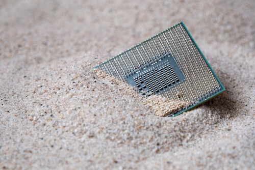
The production of a microchip starts with the extraction of silicon, one of the most abundant elements in the Earth's crust. Here, it occurs as silicon dioxide (SiO2), which is abundant in quartz sand. Quartz sand consists of approximately 95% pure quartz grains with a high SiO2 content.
- Silicon reduction: from quartz sand to pure silicon
Silicon reduction is the process of converting silicon dioxide into pure silicon. In this process, carbon is added to the quartz sand and the oxygen is dissociated with an electrothermic procedure. The result is raw silicon, which, however, requires further purification in order to be used as a base material for chip production.
In the following, you will find the next steps for the extraction and processing of silicon for microchip manufacturing. - Highly pure silicon: purification and crystal formation
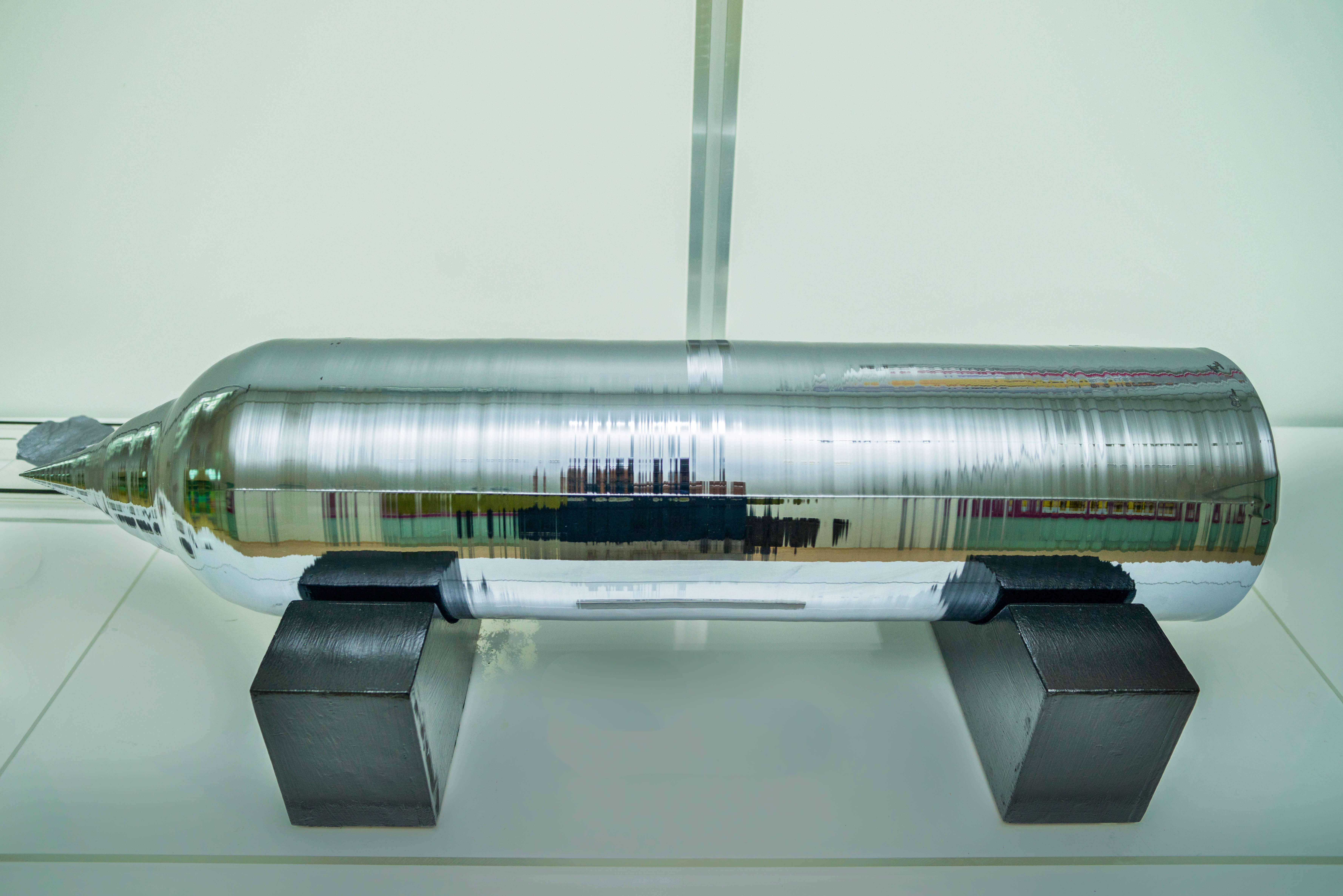
The raw silicon obtained from the previous process undergoes further purification to remove the last impurities and to ensure the required purity for chip production. By controlled melting and pulling, the silicon is then converted into a long cylindrical crystalline silicon ingot (Figure 1 - Image 1). This is sliced into thin wafers, which serve as the base for chip production. Common wafer sizes for these wafers are 100 mm, 150 mm, 200 mm, and 300 mm. The larger the wafer, the more efficient the production, as more chips can be placed on one wafer.
Figure 1: From the wafer blank to chip - Photolithography and etching: pattern creation on the wafer
Subsequently, the wafers are structured using a complex process combining photolithography and etching (Figure 1 - Images 2 and 3). Photolithography involves applying a photosensitive coating - the photoresist - to the wafer and exposing it to light, thus creating a specific pattern. Then, the exposed photoresist is developed to fix the pattern. After that, the unprotected areas of the wafer are removed by etching and the desired structures are created. - Doping and diffusion: generation of semiconductor areas
To achieve specific electrical properties, the chips are modified through doping with foreign atoms. This is done by introducing targeted impurities into the crystal lattice structure of the silicon through diffusion or ion implantation, thus generating the desired semiconductor areas (p- or n-doped areas) (Figure 1 - Image 4). A variety of test methods are then used to check the success of this process (Figure 1 - Image 5).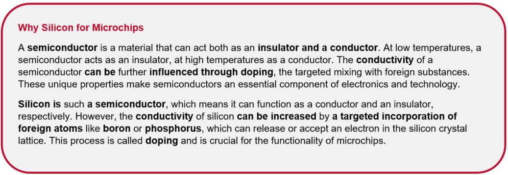
- Metallization and packaging of microchips
Once the semiconductor structures have been generated, the microchips are metallized to establish electrical connections. For this, extremely thin layers of metals such as aluminum or copper are applied to the chip and etched into the desired conductor paths. Finally, the chips are packed in protective housings (packaging) that shield them from external influences like moisture and mechanical stress (Figure 1 - Image 6).
Microchips – masterpieces of technology
From sand grain to microchips – this journey is a fascinating example of the capabilities of modern technology. The manufacturing of microchips requires an interplay of highly complex processes and technologies, in order to be able to generate tiny structures with the highest precision. The continuous development of silicon processing contributes to the ongoing improvement of the performance and versatility of electronic devices, thus paving the way for innovative applications.
Content Information

Editor: RoodMicrotec GmbH
Source: The text is based on information from RoodMicrotec GmbH.
Copyright: All images, videos and audio files published in this article are subject to copyright. Reproduction in whole or in part is not permitted without the written permission of RoodMicrotec GmbH.
For further information or inquiries about a joint cooperation, please contact